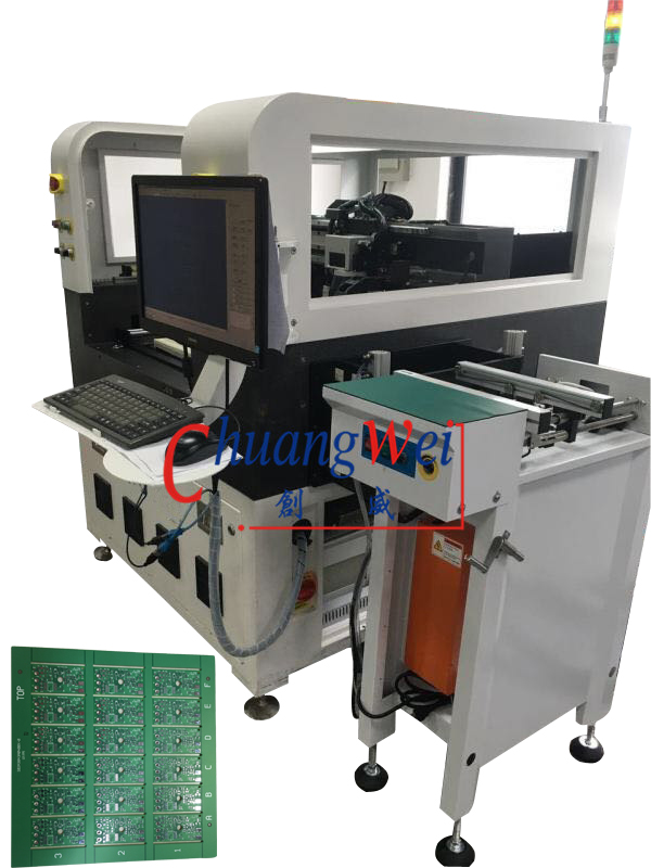
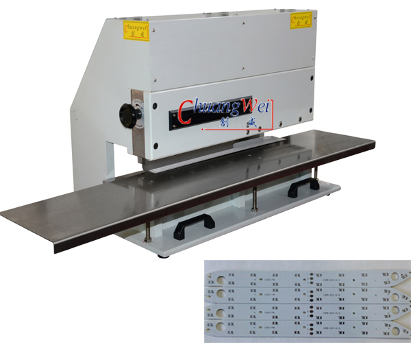
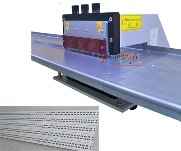
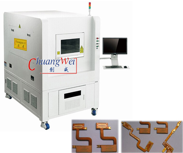
Laser PCB Separator with Different Laser Source 10/12/15/18W
PCB depaneling (singulation) laser machines and systems have been gaining popularity over recent years. Mechanical depanaling/singulation is done with routing, die cutting, and dicing saw methods. However, as the boards get smaller, thinner, flexible, and more sophisticated, those methods produce even more exaggerated mechanical stress to the parts. Large boards with heavy substrates absorb these stresses better, while these methods used on ever-shrinking and complex boards can result in breakage. This brings lower throughput, along with the added costs of tooling and waste removal associated with mechanical methods.
Increasingly, flexible circuits are found in the PCB industry, and they also present challenges to the old methods. Delicate systems reside on these boards and non-laser methods struggle to cut them without damaging the sensitive circuitry. A non-contact depaneling method is required and lasers provide a highly precise way of singulation without any risk of harming them, regardless of substrate.
Lasers, on the other hand, are gaining control of the PCB depaneling/singulation market due to higher precision, lower stress on the parts, and higher throughput. Laser depaneling can be applied to a variety of applications with a simple change in settings. There is no bit or blade sharpening, lead time reordering dies and parts, or cracked/broken edges due to torque on the substrate. Application of lasers in PCB depaneling is dynamic and a non-contact process.
| Parameter | ||
|
Technical parameters |
Main body of laser | 1480mm*1360mm*1412 mm |
| Weight of the | 1500Kg | |
| Power | AC220 V | |
| Laser | 355 nm | |
| Laser |
Optowave 10W(US) |
|
| Material | ≤1.2 mm | |
| Precisio | ±20 μm | |
| Platfor | ±2 μm | |
| Platform | ±2 μm | |
| Working area | 600*450 mm | |
| Maximum | 3 KW | |
| Vibrating | CTI(US) | |
| Power | AC220 V | |
| Diameter | 20±5 μm | |
| Ambient | 20±2 ℃ | |
| Ambient | <60 % | |
| The Machine | Marble | |
More information welcome to contact us:
WhatsApp/Wechat(Bunny): +86 136 8490 4990
www.pcb-soldering.com
Email:s5@smtfly.com
www.pcb-depanelizer.com
ChuangWei Electronic Equipment Manufactory
Contact: Bunny
Phone: /Wechat/Whatapp: +86 136 8490 4990
Tel: 86-0769-82784046
Company: Dongguan Chuangwei Electronic Equipment Manufactory
Add: Building 2, Gang Hua Xing Industrial Park, Chongqing Road, Fuyong Town, Shenzhen, China 518103
 Amy
Amy Li
Li