
Depaneling is a step easily overlooked in the printed circuit board (pcb) manufacturing process. A great board design, flawless circuit etching, and perfectly placed components mean nothing if individual pcbs cannot be separated from a panel without damaging components, solder joints, or the board itself. Conventional depaneling methods such as pcb punching, pcb depaneling, and routing impose levels of mechanical stress that exacerbate these issues, leaving a substantial amount of profit in the depaneling line’s waste bin.
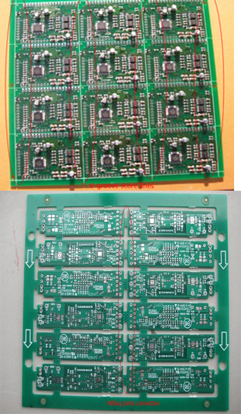
Chuangwei depaneling solution covers pcb punching, pcb depaneling, and routing for different connecting ways of panels, such as milling joints connecting, pre-scored panels different design with FPC, FR1, FR4, CEM1, CEM3, MCPCB material.
Choose Chuangwei, will give you an surprise!
By the way, Below as our information:
Weclome to visit us!
Contact: Bunny
Phone: /Wechat/Whatapp: +86 136 8490 4990
Tel: 86-0769-82784046
Company: Dongguan Chuangwei Electronic Equipment Manufactory
Add: Building 2, Gang Hua Xing Industrial Park, Chongqing Road, Fuyong Town, Shenzhen, China 518103
 Amy
Amy Li
Li